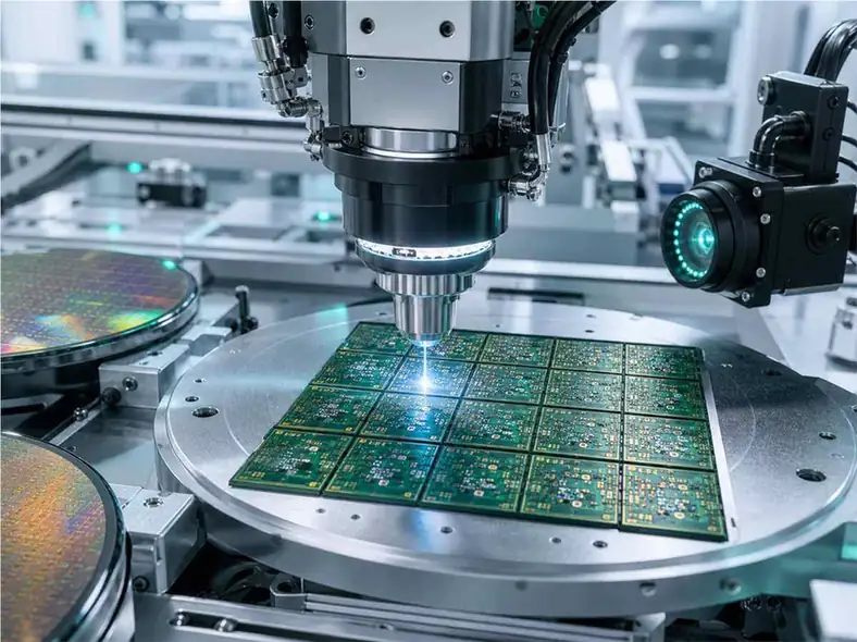
Electronics and semiconductor laser processing

Industrial Laser Applications for Electronics and Semiconductor

Industry Applications / Electronics and Semiconductor

High-contrast, low-damage, traceable processing on tiny parts

Electronics and semiconductor products keep shrinking while surfaces become more complex and data density increases. Lasers support marking, cutting, drilling, and cleaning for PCB, chips, ceramic substrates, connectors, and precision components.

Electronics and semiconductor laser processing
Micro features
Fit for fine lines, small holes, and thin materials
Low consumables
Reduce ink, tools, and mechanical dies
Readable traceability
Verify QR, DataMatrix, and serial codes inline
Clean integration
Combine extraction, vision, and automated loading
Core Processes

Common Laser Applications in Electronics and Semiconductor

Based on material, cycle time, appearance, and traceability requirements in electronics and semiconductor manufacturing, laser systems combine cutting, welding, marking, cleaning, micromachining, and automated inspection.

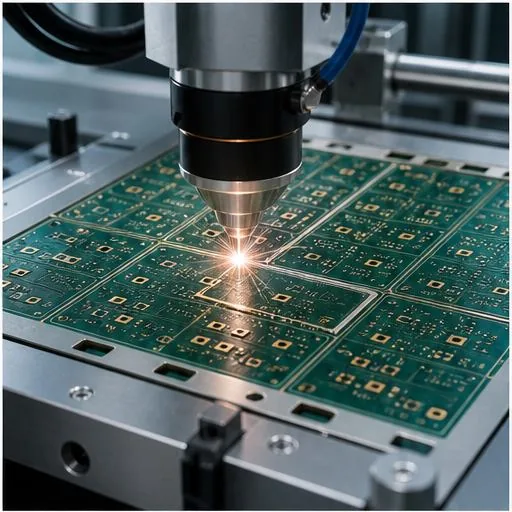
PCB cutting and coverlay opening

PCB cutting and coverlay opening

Process PCB, FPC, coverlay, and local openings.

  • Build stable parameters and reusable recipes for pcb cutting and coverlay opening.
  • Combine vision positioning, fixtures, and automated handling for consistency.
  • Scale from sample validation to automated production.
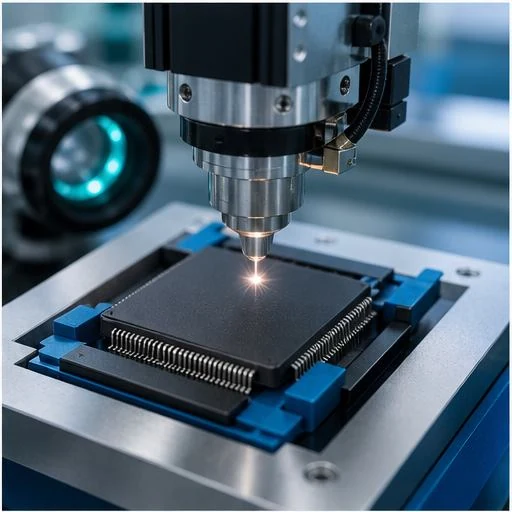
Chip and package marking

Chip and package marking

Clear permanent marks on packages, modules, and miniature components.

  • Build stable parameters and reusable recipes for chip and package marking.
  • Combine vision positioning, fixtures, and automated handling for consistency.
  • Scale from sample validation to automated production.
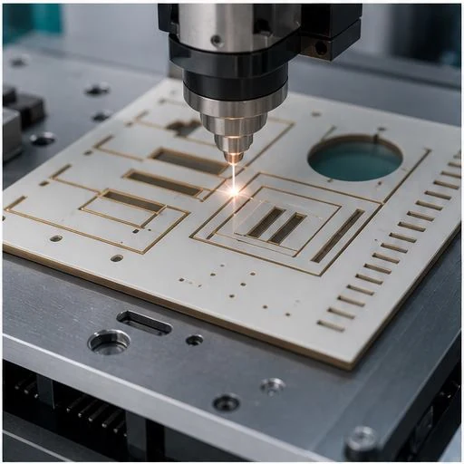
Ceramic and substrate cutting

Ceramic and substrate cutting

Machine ceramic sheets, insulating parts, and hard brittle materials.

  • Build stable parameters and reusable recipes for ceramic and substrate cutting.
  • Combine vision positioning, fixtures, and automated handling for consistency.
  • Scale from sample validation to automated production.
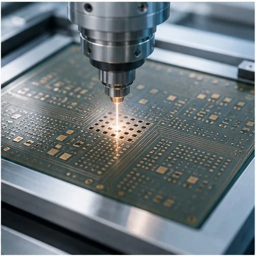
Micro drilling and precision processing

Micro drilling and precision processing

Create small holes, slots, textures, and local layer removal.

  • Build stable parameters and reusable recipes for micro drilling and precision processing.
  • Combine vision positioning, fixtures, and automated handling for consistency.
  • Scale from sample validation to automated production.
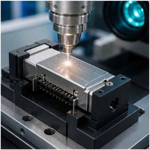
Connector and housing marking

Connector and housing marking

Mark traceability codes on plastic, metal, and coated surfaces.

  • Build stable parameters and reusable recipes for connector and housing marking.
  • Combine vision positioning, fixtures, and automated handling for consistency.
  • Scale from sample validation to automated production.
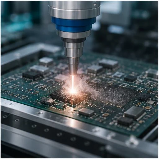
Local cleaning and layer removal

Local cleaning and layer removal

Remove oxides, coatings, residues, or local contamination.

  • Build stable parameters and reusable recipes for local cleaning and layer removal.
  • Combine vision positioning, fixtures, and automated handling for consistency.
  • Scale from sample validation to automated production.
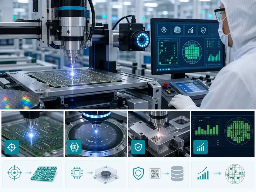
Solution Value

Laser value in Electronics and Semiconductor comes from process, automation, and data working together

A single laser process solves the operation, while production teams care about takt time, yield, changeover, and traceability. Cyanbox combines laser, vision, motion, fixtures, and software interfaces into practical cells.

Electronics and semiconductor laser processing

Contact-free processing

Reduce mechanical stress, tool wear, and secondary damage for high-appearance precision parts.

Traceability loop

Generate marks from orders, batches, or inspection results and write records back to production systems.

Automation integration

Connect robots, conveyors, rotary tables, bowl feeders, and vision positioning for continuous production.

Process quality control

Turn process know-how into repeatable standards through recipes, inline inspection, and data upload.

Implementation Path

From sample validation to Electronics and Semiconductor production cells

Validate material response, process window, and takt target first, then define laser source, vision, fixtures, extraction, safety guarding, and data interfaces.

01

Requirement and sample review

Confirm material, dimensions, surface condition, cycle time, marking or processing goals, and site safety boundaries.

02

Sample testing and process window

Validate contrast, kerf, heat impact, cleanliness, code readability, or weld quality through sample trials.

03

Cell and fixture design

Plan optics, guarding, loading, fixtures, fume extraction, and maintenance access for the production cell.

04

Vision and data integration

Connect cameras, code readers, MES / ERP, recipe control, and quality records for traceable production.

05

Ramp-up and optimization

Complete installation, training, cycle-time tuning, process standardization, and ongoing support.

Use Cases

Priority Production Areas for Electronics and Semiconductor

When products need permanent marks, precision processing, flexible changeover, or more stable appearance quality, laser solutions usually show clearer return.

PCB / PCBA

Circuit boards, flexible boards, modules, and assemblies.

Semiconductor packaging

Chip packages, power modules, ceramic substrates, and carriers.

Consumer electronics

Phones, wearables, smart hardware, and connector components.

Precision small parts

Sensors, miniature structures, thin sheets, and insulating parts.

Evaluating laser processing or automation cells for Electronics and Semiconductor?

Share material, part size, process goals, target cycle time, and current pain points. We can help evaluate laser source, vision, fixtures, and automation integration.